 11/12/2015
 12:00 h
 ICIQ Auditorium
- Lecturer: Dr. Concha Bosch Navarro
- University: The University of Warwick (United Kingdom)
- Sponsored by:

Graphene and its Role as Support in Transmission Electron Microscopy
Graphene can be defined as a single layer of hybridized sp2 carbon atoms arranged in a honeycomb lattice distribution. Their unique physical characteristics which include high thermal and electrical conductivity, optical transparency and unprecedented mechanical strength, place it as the most promising next-generation electronic material. In addition, its enormous surface area (2630 m2 g-1) together with its chemical versatility provides with a unique 2D platform from which creating nanoscale hybrid materials and composites with enhanced properties suitable for different applications.
The increasing diversity of nanoscale structures requires, however, techniques capable of resolving subtle structural fluctuations and interactions between molecular species on an atomic scale. Transmission electron microscopy (TEM) is an imaging technique that permits direct investigation of the intimate structural details of a wide variety of nanomaterials, especially carbon based nanomaterials, including carbon nanotubes, graphene and graphene derivatives. Recent advances have led to the extensive use of aberration corrected transmission electron microscopes (ac-TEMs), which permit atomic resolution at low electron accelerating voltages and have made great advances in structural elucidation of carbon based materials.
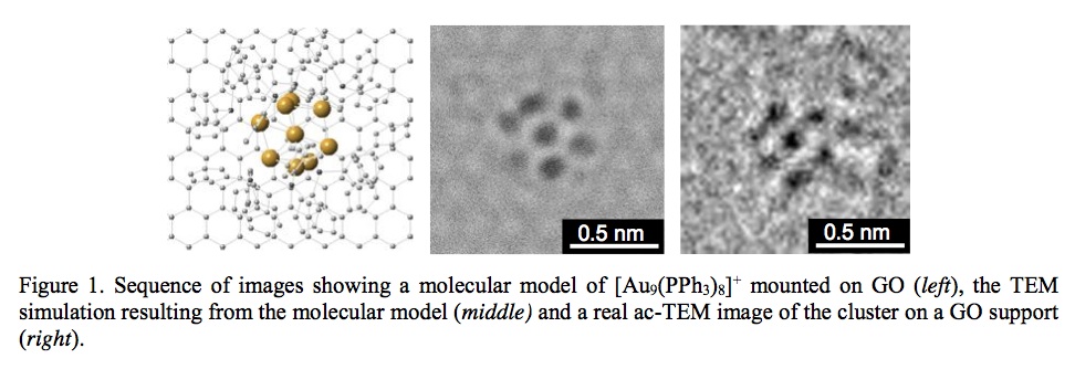
A key aspect for the rapid development of ac-TEM has been the emergence of electron transparent carbon-based supports that are compatible with the lowering of the accelerating voltage to ≤ 80 kV. Thus, carbon nanotubes and fullerenes have been widely used as molecular cages to isolate and image a wide variety of molecular scale nanostructures. An alternative is the use of ultrathin 2D supports such as graphene, graphene oxide (GO) or boron nitride, which provide an atomically thin electron transparent periodic support that serves as internal calibration, and enables tracking of molecular motion. The use on GO supports allows us to achieve atomic resolution by ac-TEM on a variety of heavy atom molecular clusters (e.g. [Au9(PPh3)8]+ or [CoSiW11O39]6-) deposited on GO (Figure 1).
Other events

Let's create a brighter future
Join our team to work with renowned researchers, tackle groundbreaking
projects and contribute to meaningful scientific advancements


