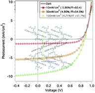
Solvent vapour annealing (SVA), which consists of exposing the active layer of organic films to a vapour of solvent directly after deposition, has been used in small molecule bulk heterojunction (SM-BHJ) solar cell devices whose active layer consisted of 3,6-bis(5-(benzofuran-2-yl)thiophen-2-yl)-2,5-bis(2-ethylhexyl)pyrrolo[3,4-c]pyrrole-1,4-dione (DPP(TBFu)2) and [6,6]-phenyl-C71-butyric acid methyl ester (PC71BM). We demonstrate that upon SVA, well-ordered crystalline domains of the DPP(TBFu)2 donor form inside the active layer, improving greatly the Fill Factor (FF) of the devices. However, SVA treatment is always accompanied by a decrease in device short circuit current (JSC). We demonstrate, using 1D and 2D XRD and AFM, that crystalline domains of DPP(TBFu)2 form in a matrix of PC71BM acceptor. The crystallinity increases with annealing time (ta) and the change in FF and JSC is directly linked to this. The X-ray single crystal structure of the DPP(TBFu)2 donor was solved and provided information of the donor’s packing in the solid state. The donor molecules were shown to pack in a herringbone arrangement and shown to form a highly texturized active layer film. We demonstrated that the ability of the donor to form large and highly texturized crystalline domains in the active layer is as equally as determining for the devices’ characteristics as the individual stacking properties of the donor in the solid state.
